


scanning electron microscopy

SEM ANALYSIS WITH EDS CAPABILITIES
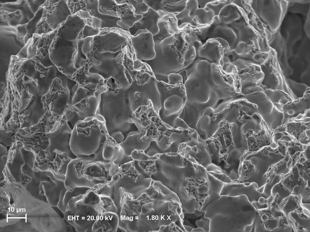
Scanning Electron Microscopy (SEM) is a powerful tool that scans a sample with an electron beam to produce a magnified image for analysis. The highly magnified images provide a powerful and effective micro analysis technique tool in failure analysis, dimensional analysis, contaminant analysis, particle analysis, and reverse engineering. Images produced by a fracture surface are often used to determine the mode and mechanism of failure.
MODERN SEM FACILITIES
Our surface analysis lab in the Dallas, TX metroplex provides top tier scanning electron microscope services, utilizing Zeiss and Jeol SEMs that include EDAX and Thermo Energy Dispersive X-ray Spectroscopy (EDS) capabilities for chemical composition.
The SEM analysis lab will allow you to view surface features at 5 to 300,000X magnification to provide you with high quality, depth of field images. When used with EDS detectors attached to each SEM, the chemical composition of surface features is quickly attained. While often used for metals and minerals, the MES beam lab includes a variable pressure system capable of analyzing non-conductive samples (such as polymers) with minimal preparation.
SEM ANALYSIS REPORTS
Upon completion of your metals testing or analysis, a comprehensive report will be provided with EDS test data, high magnification images, referenced test specification, and interpretation from a materials engineer.
THE SEM ANALYSIS ADVANTAGE
Scanning Electron Microscopy (SEM) is an essential tool in failure analysis, helping engineers and scientists investigate and understand the reasons behind the failure of materials and components.
Here's how SEM is used in failure analysis:
Detailed Surface Imaging: SEM provides highly detailed images of the failed material's surface, allowing analysts to examine the fracture surface, cracks, corrosion, or any other visible damage. The high magnification and resolution of SEM help reveal the morphology and topography of the failure features.
Microstructural Analysis: SEM enables the examination of the microstructure of the material. By preparing the sample appropriately, such as through polishing and etching, analysts can study the grain structure, phase distribution, and any microstructural abnormalities that might contribute to the failure.
Elemental Composition Analysis: SEM can perform energy-dispersive X-ray spectroscopy (EDS) or X-ray microanalysis, which helps identify and quantify the elemental composition of the failed material. This analysis can reveal the presence of impurities, contaminants, or variations in alloy composition that might have played a role in the failure.
Fracture Surface Analysis: SEM allows investigators to analyze the fracture surfaces of failed components. By examining the fracture mode, crack propagation patterns, and the presence of specific features like fatigue striations or ductile tearing, analysts can determine the failure mechanism and understand if it was due to overload, fatigue, or other factors.
Corrosion Analysis: In cases of corrosion-related failures, SEM can provide valuable information about the corrosion products, corrosion morphology, and the extent of corrosion damage. This helps identify the corrosive agents, assess the corrosion mechanisms, and guide preventive measures.
Foreign Object Analysis: Sometimes, the presence of foreign objects can lead to component failure. SEM enables the examination and identification of foreign particles or contaminants on the surface or within the material, providing insights into their origin and potential impact on the failure.
By utilizing SEM in failure analysis, engineers and scientists can gain a deeper understanding of the underlying causes of failures, aiding in the improvement of materials, design, manufacturing processes, and preventive measures to avoid future failures. Our superior instrumentation allows us to provide exemplary service at very competitive prices.
CAPABILITIES
High Magnification Imaging – up to 300,000x
Examination of fractured surfaces
Semi-quantitative chemical analysis by EDS
Evaluation of crystallographic orientation
Low cost chemical and contaminant identification
Analysis of metals, polymers, and minerals
SPECIFICATIONS
ASTM B748 - Metallic Coating Thickness Measurements
ASTM E1508 - EDS Analysis
SAMPLE REQUIREMENTS
Sample Size – up to 8 in. diameter and 3 in. in height